-
关注商城

关注官方微信
关注官方微信

销售咨询
技术支持

联系客服


 购前提示 |
常用产品货期为1-2天,非常用产品为一周; 进口产品、贵金属产品、订制规格产品,价格、货期影响因素较多。 关于货期、价格、质量规格等问题采购前,请于客服沟通。 |
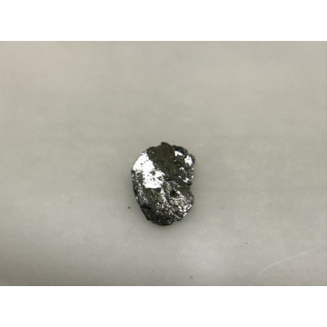
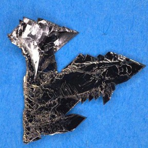
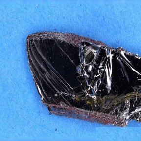
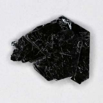
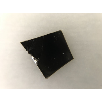
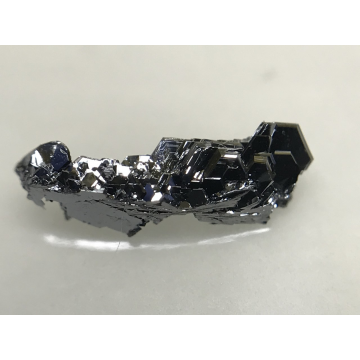
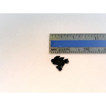
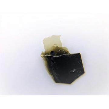
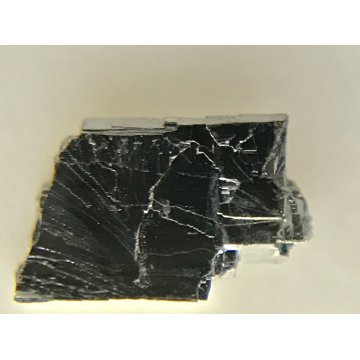
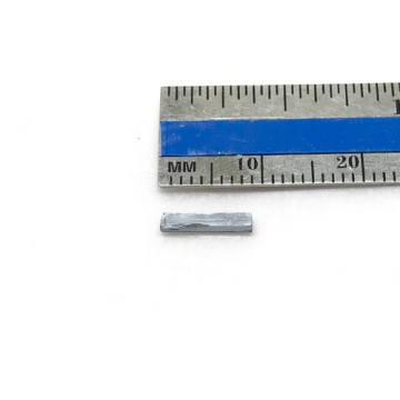
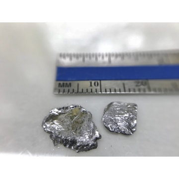
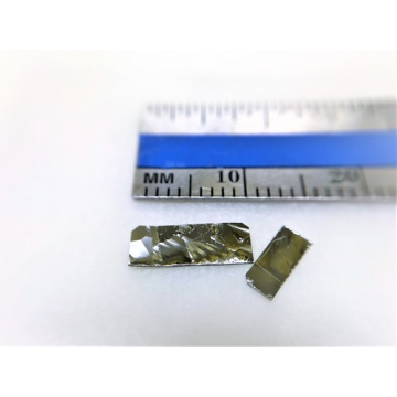
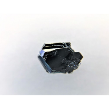
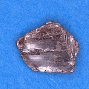
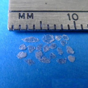
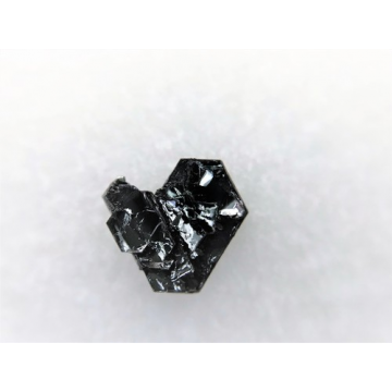
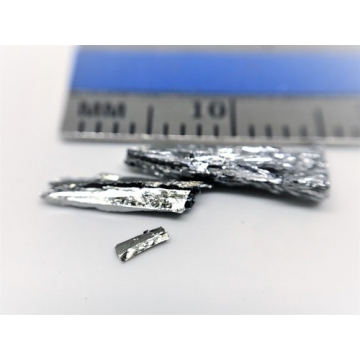
Synthetic single crystal Tin lead disulfide (PbSnS₂) is a special member of layered transitional metal dichalcogenides. Similar to MoS₂, MoSe₂, WS₂, and WSe₂, adjacent layers are weakly coupled to each other and can be easily exfoliated (see images) and isolated down to monolayers. In the bulk it possesses 1.45 eV band gap. Physical properties of monolayer PbSnS₂ are unknown both theoretically and experimentally. The first monolayer PbSnS₂ has been synthesized at our facilities in late 2012 and the bulk crystals are perfected after two (2) years of development process.
Crystals are up to 10mmx10mm in size and highly crystalline. Ready for exfoliation to yield monolayers.
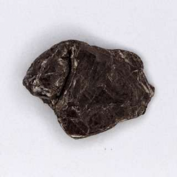
Differences between the synthetic and the natural PbSnS₂;
- Purity and magnetic properties: The synthetic PbSnS₂ is 99.995% pure. Diamagnetic semiconductor. The natural PbSnS₂ is 98-99% pure and contains various impurities including anti-ferromagnetic iron oxides, ferromagnetic iron and nickel complexes. Therefore, natural PbSnS₂ is ferromagnetic semiconductor.
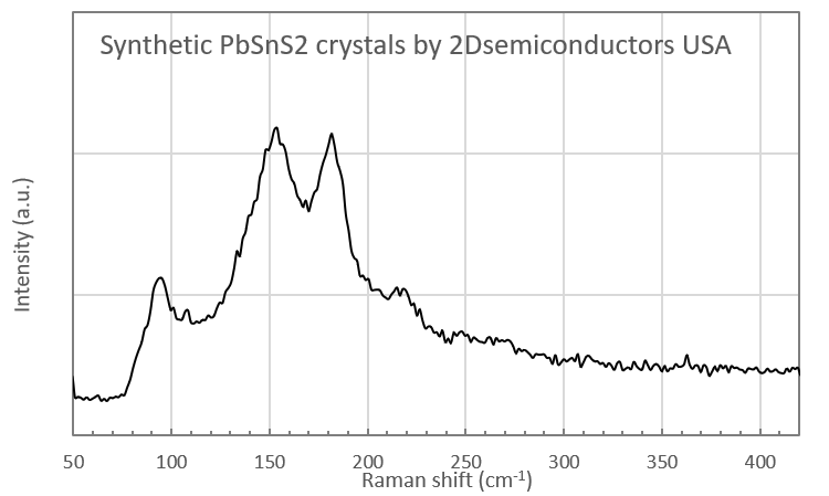
- Defect profile and Raman spectrum: The Synthetic PbSnS₂ contains least amount of defects. Therefore, synthetic PbSnS₂ has much sharper Raman peaks.
- Sub-band gap: Natural PbSnS₂ possesses defect induced sub-band gaps and enhanced exciton-phonon interaction.
- Mechanical differences: Natural PbSnS₂ is more fragile compared to synthetic PbSnS₂. The mechanical stiffness and fragility stem from the increased density of defects.
- Electrical properties: Natural crystals have smaller grain sizes and the transport is mostly dominated by the variable-hopping and grain boundary scattering. Synthetic materials possess conventional lightly-doped semiconductor behavior.
Raman spectrum collected from PbSnS2 crystals


宝贝与描述相符
5