-
关注商城

关注官方微信
关注官方微信

销售咨询
技术支持

联系客服


 购前提示 |
常用产品货期为1-2天,非常用产品为一周; 进口产品、贵金属产品、订制规格产品,价格、货期影响因素较多。 关于货期、价格、质量规格等问题采购前,请于客服沟通。 |
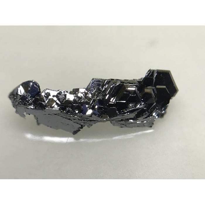
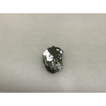
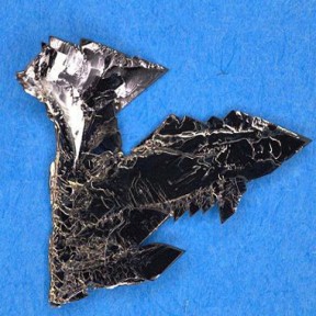
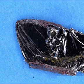
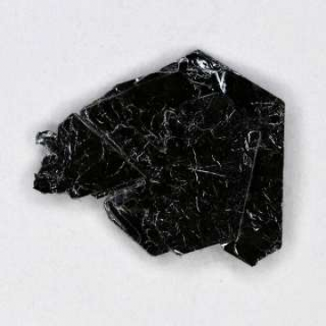
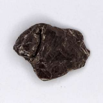
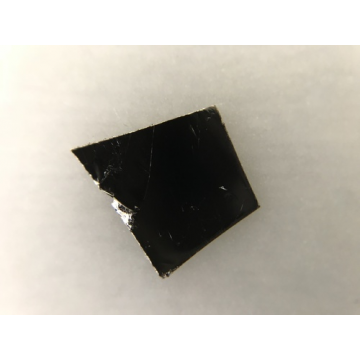
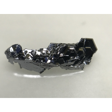
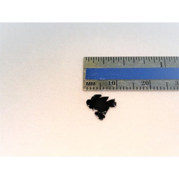
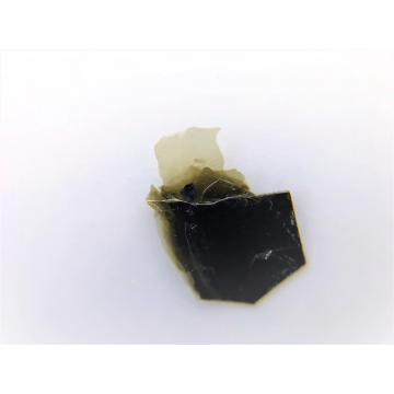
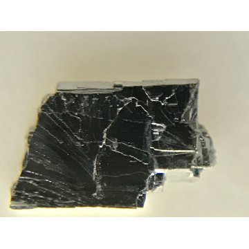
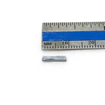
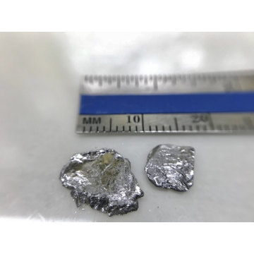
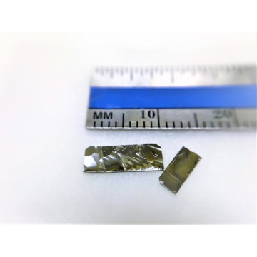
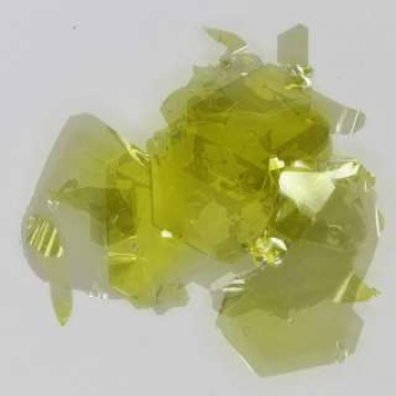
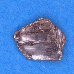
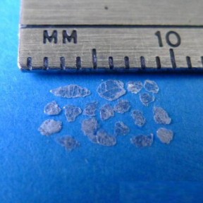
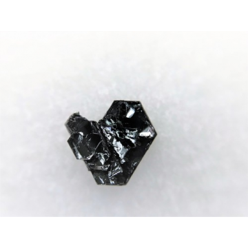
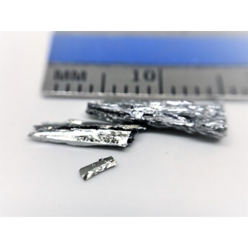
Single crystal ReS₂ (Rhenium disulfide) crystals are developed at our facilities using chemical vapor transport or flux zone technique methods after 9 years of growth optimization to ensure anisotropic properties. Our ReS2 crystals display impressive structural anisotropy from bulk down to monolayers as evidenced by TEM and angle resolved Raman spectroscopy measurements (see XRD, TEM, Raman, PL, and other figures below). Crystals are rather large in size, perfectly layered, and ready for exfoliation. Our R&D team also provides you with transfer technique to boost your monolayer yield rate up to 95%. If your research needs doped ReS2 crystals, we can introduce Mo, Au, Nb, and other dopants.
To see our CVD ReS2 monolayer products, please go to CVD ReS2 website [click here]
Typical characteristics of ReS2 crystals from 2Dsemiconductors

Growth method matters> Flux zone or CVT growth method? Contamination of halides and point defects in layered crystals are well known cause for their reduced electronic mobility, reduced anisotropic response, poor e-h recombination, low-PL emission, and lower optical absorption. Flux zone technique is a halide free technique used for synthesizing truly semiconductor grade vdW crystals. This method distinguishes itself from chemical vapor transport (CVT) technique in the following regard: CVT is a quick (~2 weeks) growth method but exhibits poor crystalline quality and the defect concentration reaches to 1E11 to 1E12 cm-2 range. In contrast, flux method takes long (~3 months) growth time, but ensures slow crystallization for perfect atomic structuring, and impurity free crystal growth with defect concentration as low as 1E9 - 1E10 cm-2. During check out just state which type of growth process is preferred. Unless otherwise stated, 2Dsemiconductors ships Flux zone crystals as a default choice.
XRD data collected from ReS2 crystals

Raman spectrum collected from ReS2 monolayers

PL spectrum collected from ReS2 on SiO2/Si substrates

SIMS purity datasets collected from ReS2 crystals

HRTEM images collected from ReS2 crystals

Please also see our new product 'Full coverage monolayer ReS2 on c-cut sapphire'.
Partial List of Publications Using This Product
D. Wolverson et,al. "Rhenium Dichalcogenides: Layered Semiconductors with Two Vertical Orientations," Nano Letters 2016, 16, 1381−1386
Ignacio Gutiérrez-Lezama et. al. "Electroluminescence from indirect band gap semiconductor ReS2" 2D Materials, Volume 3, Number 4
Manish Chhowalla, "Two-dimensional semiconductors for transistors" Nature Reviews Materials 1, Article number: 16052 (2016) doi:10.1038/natrevmats.2016.52
Q. Cui et. al. "Coherent Control of Nanoscale Ballistic Currents in Transition Metal Dichalcogenide ReS2" ACS Nano 10.1021/acsnano.5b01111 (2015)
X-F. Qiao et.al. "Polytypism and unexpected strong interlayer coupling in two-dimensional layered ReS2" Nanoscale, 2016, 8, 8324 (2016)
D. Wolverson et.al. "Raman Spectra of Monolayer, Few-Layer, and Bulk ReSe2: An Anisotropic Layered Semiconductor" ACS Nano, 2014, 8 (11), pp 11154–11164
E. Lorchat et.al. "Splitting of Interlayer Shear Modes and Photon Energy Dependent Anisotropic Raman Response in N-Layer ReSe2 and ReS2" ACS Nano, 2016, 10 (2), pp 2752–2760


宝贝与描述相符
5