-
关注商城

关注官方微信
关注官方微信

销售咨询
技术支持

联系客服


 购前提示 |
常用产品货期为1-2天,非常用产品为一周; 进口产品、贵金属产品、订制规格产品,价格、货期影响因素较多。 关于货期、价格、质量规格等问题采购前,请于客服沟通。 |
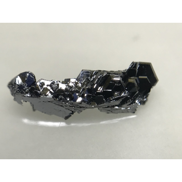
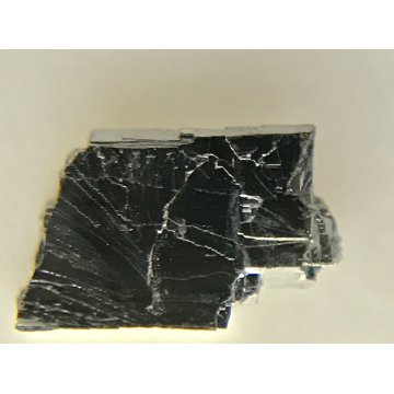
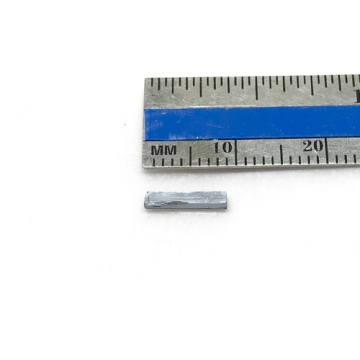
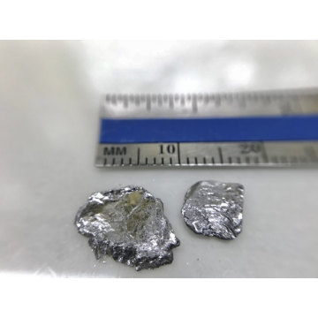
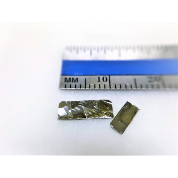
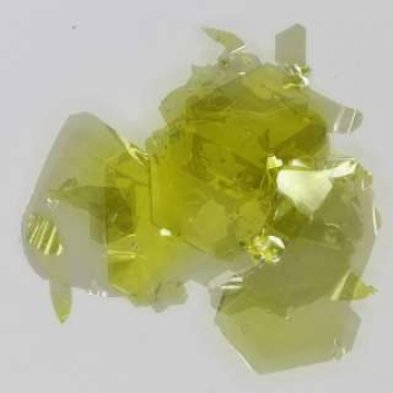
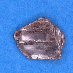
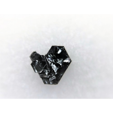
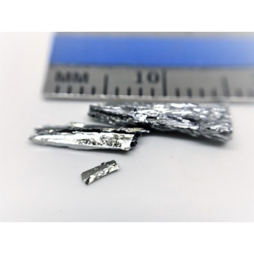
Hexagonal boron nitride is a semiconductor with a direct band gap of ~5.9 eV and has been used extensively as an insulator for the production of ultrahigh mobility 2D heterostructures composed of various types of 2D semiconductors (e.g. WSe2, MoSe2, etc). The layers are stacked together via van der Waals interactions and can be exfoliated into thin 2D layers, down to monolayer h-BN. To buy hexagonal boron nitride crystals please click here.
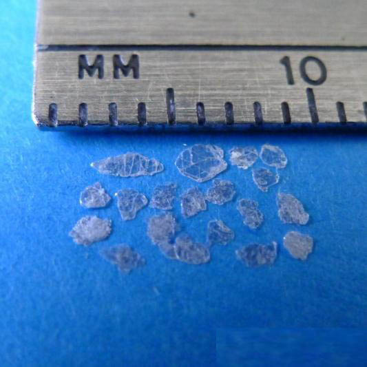
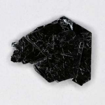
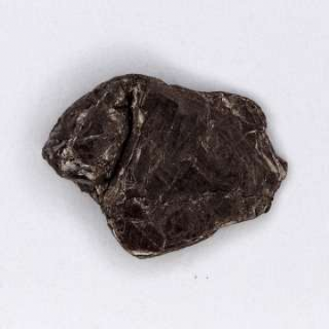
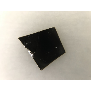
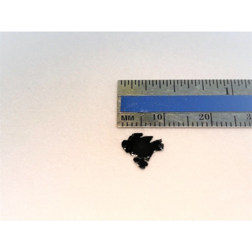
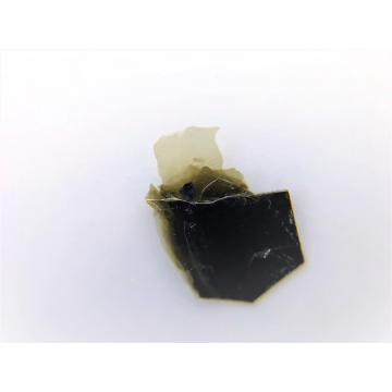
The h-BN crystals from HQ Graphene have a typical lateral size of ~0.1 cm and are transparent. The monocrystalline h-BN is an excellent insulator which is represented by its very large breakdown voltage (>0.4 V/nm). Large area size h-BN single crystals can be can be exfoliated onto a substrate (eg. SiO2, quartz, polymer, etc). Sizes range up to ~100 μm for crystals with a thickness of a few tens on nm thick. A selection of peer review publications on the hexagonal Boron Nitride we sell can be found below.
h-BN crystal properties
| Crystal size | ~1 mm |
| Electrical properties | Insulator/Semiconductor |
| Crystal structure | Hexagonal |
| Unit cell parameters | a = b = 0.2502 nm, c = 0.6617 nm, α = β = 90°, γ = 120° |
| Type | Synthetic |
| Purity | Grade A |
| Characterized by | XRD, Raman, EDX |
| More information? | Please contact us by email or phone |
XRD: single crystal and powder X-ray diffraction (D8 Venture Bruker and D8 Advance Bruker)
EDX: Energy-dispersive X-ray spectroscopy for stoichiometric analysis
Raman: 785nm Raman system
Click on an image to zoom
 X-ray diffraction on a hexagonal boron nitride single crystal aligned along the (001) plane. XRD was performed at room temperature using a D8 Venture Bruker. The 4 XRD peaks correspond, from left to right, to (00l) with l = 1, 2, 3
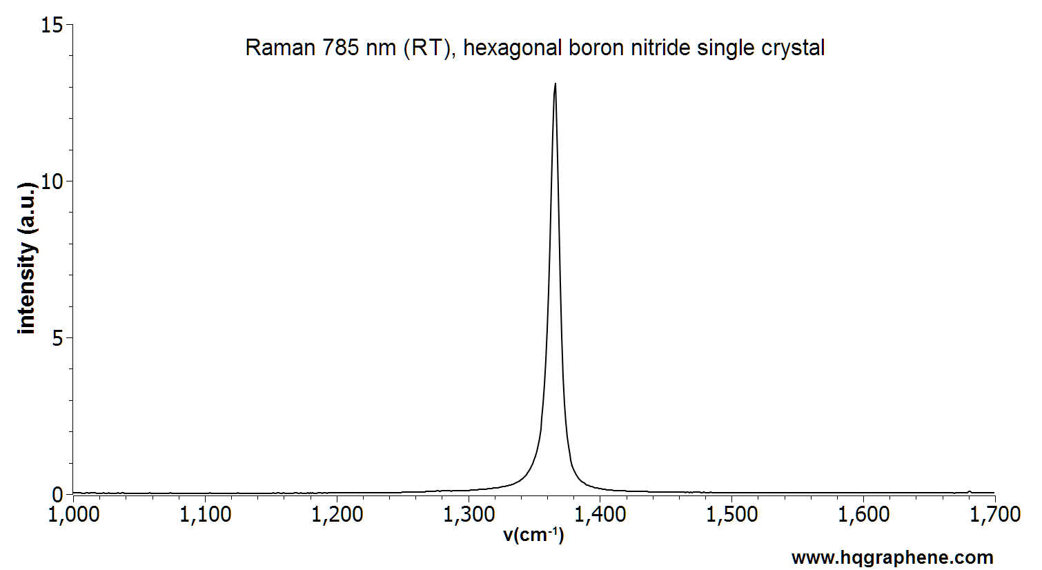 Raman spectrum of a single crystal hexagonal boron nitride (h-BN). Measurement was performed with a 785nm Raman system at room temperature.
![]() Device at left side: Fabrication of a high mobiltity bilayer graphene. This field effect transistor is fabricated using the polymer 2D_CL_PC . The device is composed out of four 2D layers. The bilayer graphene is encapsulated between two hexagonal boron nitride crystals (h-BN). The fourth layer is a thin layer of graphite (HOPG) which is used as a backgate. Scale bar is 20μm. Device at right side: This device is similar to the one at the left side, here we added on the top hexagonal boron nitride layer a gold electrode in order to apply a top gate voltage to the hBN encapsulated bilayer graphene. Scale bar is 20μm
Device at left side: Fabrication of a high mobiltity bilayer graphene. This field effect transistor is fabricated using the polymer 2D_CL_PC . The device is composed out of four 2D layers. The bilayer graphene is encapsulated between two hexagonal boron nitride crystals (h-BN). The fourth layer is a thin layer of graphite (HOPG) which is used as a backgate. Scale bar is 20μm. Device at right side: This device is similar to the one at the left side, here we added on the top hexagonal boron nitride layer a gold electrode in order to apply a top gate voltage to the hBN encapsulated bilayer graphene. Scale bar is 20μm


宝贝与描述相符
5