-
关注商城

关注官方微信
关注官方微信

销售咨询
技术支持

联系客服


 购前提示 |
常用产品货期为1-2天,非常用产品为一周; 进口产品、贵金属产品、订制规格产品,价格、货期影响因素较多。 关于货期、价格、质量规格等问题采购前,请于客服沟通。 |
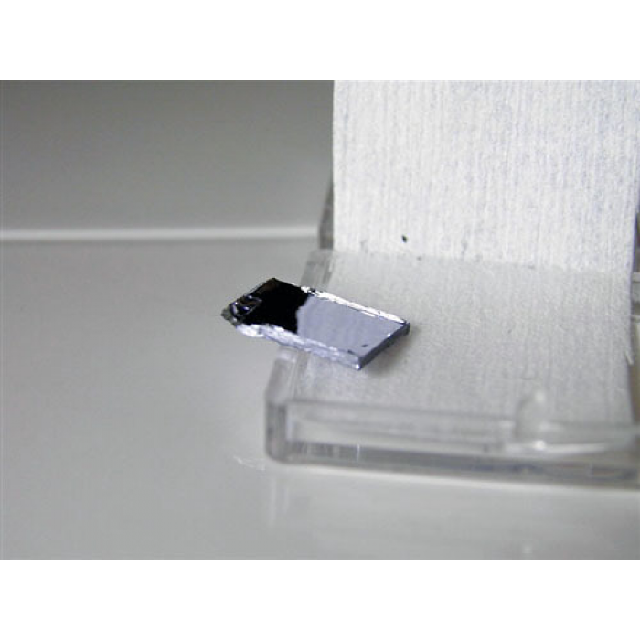
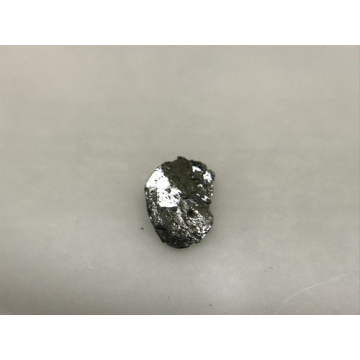
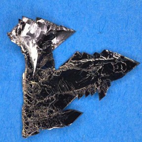
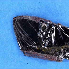
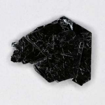
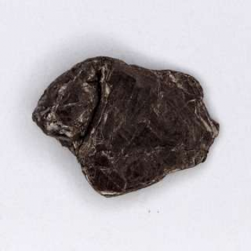
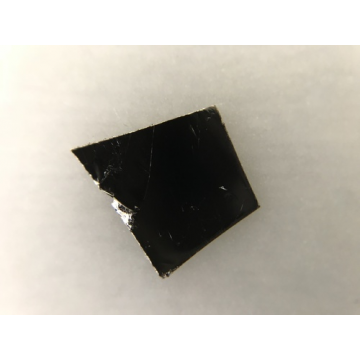
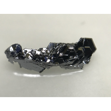
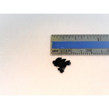
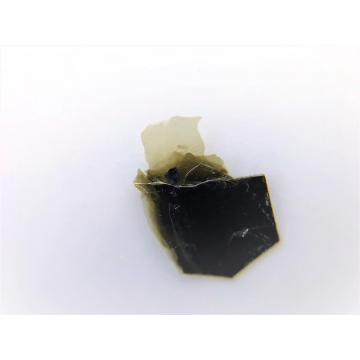
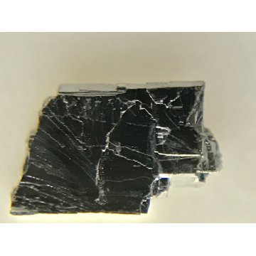
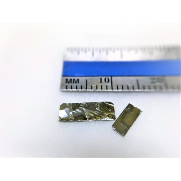
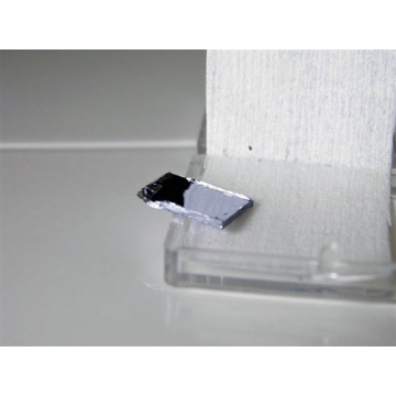
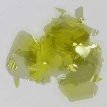
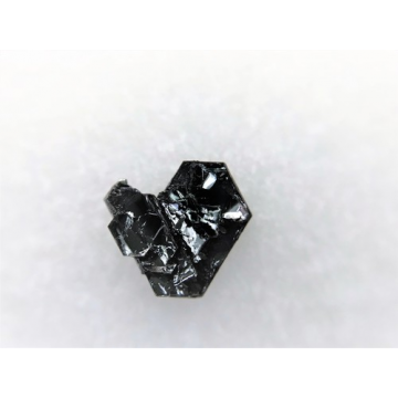
Single crystal highly oriented synthetic 2H-phase MoS2 crystals have been developed at our facilities in the USA starting from the powder making to crystallization. Our crystals are well-known for its low defect density, ultra-flat surfaces, and high crystallinity. Synthetic MoS2 samples have excellent layer by layer stacking with very small (0.3 degree) mosaic spread which enables you to exfoliate large monolayers with minimal amount of effort. Synthetic MoS2 is an indirect gap semiconductor (1.2 eV) but becomes highly luminescent in the monolayer from at 1.9 eV (quasi-particle / optical band gap). Synthetic MoS2 crystals are superior to natural MoS2 in in defects, electronic and optical performance, purity, and surface smoothness. Please also see our nature small, medium, and large MoS2 crystals.
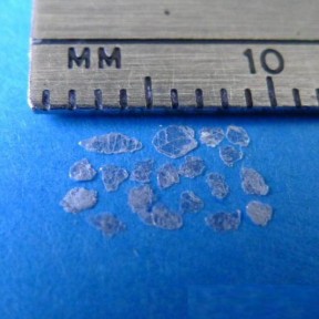
Characteristics of SnS2 crystals
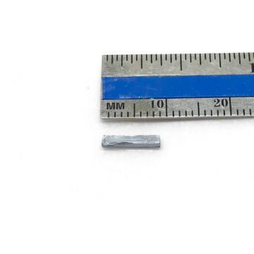
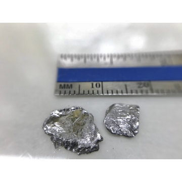
| Crystal size | 10mm or larger |
| Material properties | Bulk: Indirect 1.2eV 1L: Direct gap 1.9 optical band gap |
| Crystal structure | Hexagonal phase (2H-phase) |
| Unit cell parameters | a=b=0.316nm, c=1.230nm,α=β=90°,γ=120° |
| Growth method | Chemical vapor transport/Optional:Flux zone growth |
| Purity | 99.9999% confirmed |
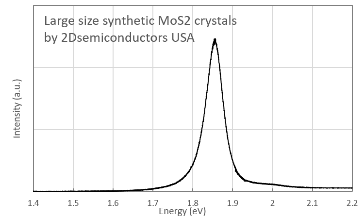
Photoluminescence spectrum from monolayer MoS2 sheets exfoliated from synthetic MoS2 crystals
Raman spectrum from synthetic MoS2 crystals

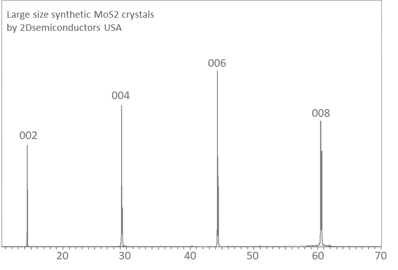
XRD data collected from synthetic MoS2 crystals
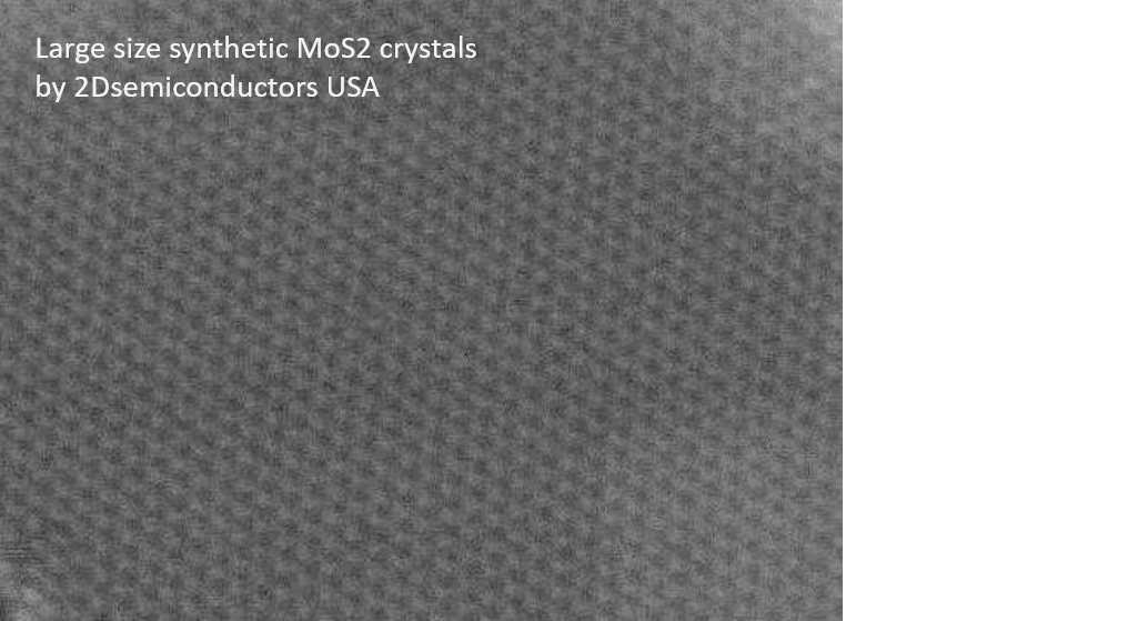
Transmission electron microscopy data collected from monolayer MoS2 sheets exfoliated from synthetic MoS2 crystals
Publications from this product
Summary: Publications from Cornell, Washington, MIT, Berkeley, Stanford, and Princeton teams at top journals like Nature, Nature Materials, Nature Communications, Nano Letters, and Advanced Materials
C. Robert, "Optical spectroscopy of excited exciton states in MoS2 monolayers in van der Waals heterostructures" Phys. Rev. Materials 2, 011001(R) (2018)
Lu Hua Li et. al. Asymmetric electric field screening in van der Waals heterostructures; Nature Communications 9, 1271 (2018) doi:10.1038/s41467-018-03592-3
X. Wang et.al. "Substrate modified thermal stability of mono- and few-layer MoS2" Nanoscale, 2018, 10, 3540-3546
L. Zhang. et.al. "Photonic-crystal exciton-polaritons in monolayer semiconductors" Nature Communications volume 9, Article number: 713 (2018)
Weigao Xu et al., "Correlated fluorescence blinking in two-dimensional semiconductor heterostructures", Nature 541, 62-67 (2017), link to article:
http://www.nature.com/nature/journal/v541/n7635/full/nature20601.html
Manish Chhowalla team "Phase-engineered low-resistance contacts for ultrathin MoS2 transistors" Nature Materials DOI: 10.1038/NMAT4080
X. Chen "Probing the electron states and metal-insulator transition mechanisms in molybdenum disulphide vertical heterostructures" Nature Communications 6, Article number: 6088 (2015) doi:10.1038/ncomms7088
Measurement of the optical dielectric function of monolayer transition-metal dichalcogenides: MoS2, MoSe2, WS2, and WSe2, Yilei Li, Alexey Chernikov, Xian Zhang, Albert Rigosi, Heather M. Hill, Arend M. van der Zande, Daniel A. Chenet, En-Min Shih, James Hone, and Tony F. Heinz; Phys. Rev. B 90, 205422 (2014)
H. Wang et.al. "Ultrafast response of monolayer molybdenum disulfide photodetector" Nature Communications 6, Article number: 8831 (2015)
Y. Jin "A Van Der Waals Homojunction: Ideal p–n Diode Behavior in MoSe2" Advanced Materials 27, 5534–5540 (2015)
Tongay et. al. "Defects activated photoluminescence in two-dimensional semiconductors: interplay between bound, charged, and free excitons" Scientific Reports 3, Article number: 2657 (2013)
X Li et al. "Determining layer number of twodimensional flakes of transition-metal dichalcogenides by the Raman intensity from substrates" Nanotechnology 27 (2016) 145704
Tongay et.al. Thermally Driven Crossover from Indirect toward Direct Bandgap in 2D Semiconductors: MoSe2 versus MoS2; Nano Letters, 2012, 12 (11), pp 5576–5580
Manish Chhowalla, "Two-dimensional semiconductors for transistors" Nature Reviews Materials 1, Article number: 16052 (2016) doi:10.1038/natrevmats.2016.52
D. Wolverson et.al. "Raman Spectra of Monolayer, Few-Layer, and Bulk ReSe2: An Anisotropic Layered Semiconductor" ACS Nano, 2014, 8 (11), pp 11154–11164
M. Yankowitz et. al. "Intrinsic Disorder in Graphene on Transition Metal Dichalcogenide Heterostructures" Nano Letters, 2015, 15 (3), pp 1925–1929
H. C. Diaz et.al. "Molecular beam epitaxy of the van der Waals heterostructure MoTe2 on MoS2: phase, thermal, and chemical stability" 2D Materials, Volume 2, Number 4 (2015)
A. Gul et.al. "Theoretical and experimental investigation of conjugation of 1,6-hexanedithiol on MoS2" Materials Research Express, 5 (3), 036415 (2018)
C. Robert "Optical spectroscopy of excited exciton states in MoS2 monolayers in van der Waals heterostructures" Phys. Rev. Materials, 2, 011001 (R)


宝贝与描述相符
5