-
关注商城

关注官方微信
关注官方微信

销售咨询
技术支持

联系客服


 购前提示 |
常用产品货期为1-2天,非常用产品为一周; 进口产品、贵金属产品、订制规格产品,价格、货期影响因素较多。 关于货期、价格、质量规格等问题采购前,请于客服沟通。 |
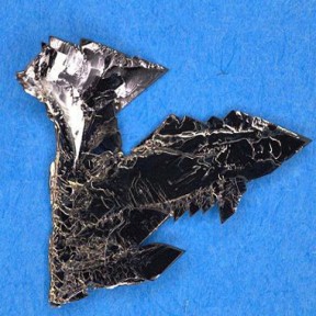
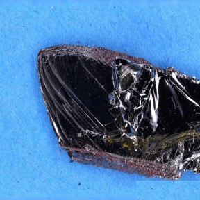
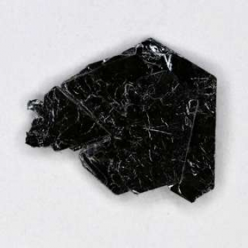
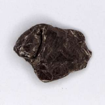
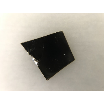
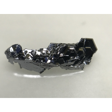
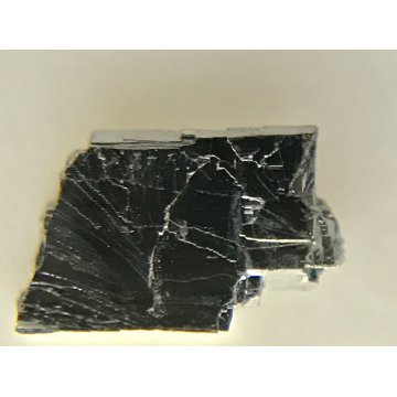
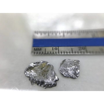
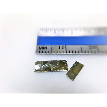
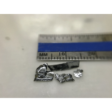
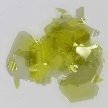
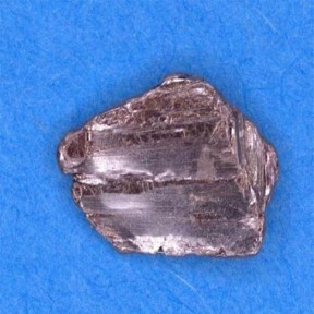
In the bulk form SnSe has band-gap at around 0.9 eV (indirect) and 1.25 direct gaps. It has layered structure (lamellar) with weak interlayer coupling, enabling to isolate down to monolayers. Each monolayer is four atoms thick (Se-Sn-Sn-Se) that is roughly 0.9-1.0 nm. At high pressures it undergo semiconductor to superconductor transition. More recently, SnSe has been shown to display world record performance for thermoelectric material efficiency.
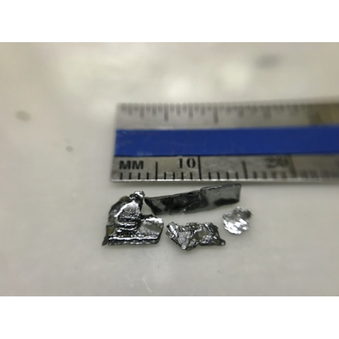
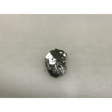
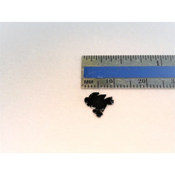
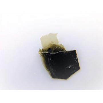
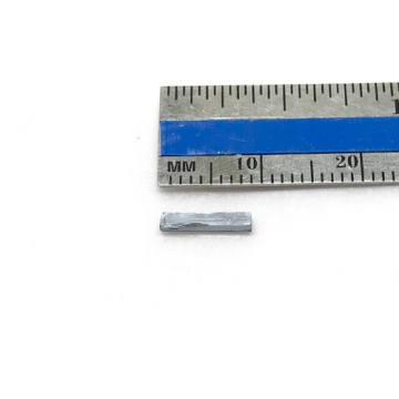
SnSe single crystal characteristics
| Crystal size | 1cm in size |
| Material properties | Thermoelectric semiconductor (anisotropic semiconductor) |
| Crystal structure | Pnma [62] |
| Unit cell parameters | a=0.421nm,b=0452nm, c=1.181nm,α=β=γ=90° |
| Growth method | Bridgman growth technique |
| Purity | 99.9999% confirmed |
Raman spectrum collected from SnSe crystals


宝贝与描述相符
5